Cadence
EECraftsman technical team members have more than ten years of experience in the application of Cadence series software to complete the development of electronic circuits. The following three typical cases are successful cases completed by our company according to different industries and different needs.
CASE ONE
A medical electronics customer of our company commissioned us to design a dental cleaning machine PCB with allegro
Number of floors: 4
Including:optical coupling isolation module, relay control module, MOS switch control circuit, temperature detection, water level detection related ADC acquisition module, ESD protection circuit, USB high-speed bus, motor fan control circuit, SPI bus and other modules
The PCB has the characteristics of multi-power system, and pays more attention to the processing of plane segmentation in the design.
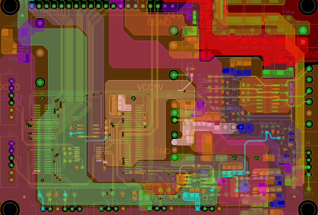
CASE TWO
An industrial equipment customer commissioned our company to complete the allegro design of an industrial analysis instrument board card, used for discharge industrial analysis and element analysis
Number of floors: 4
Including:USB high-speed serial port bus, LVDS high-speed interface, MIPI high-speed interface, high-precision DC-DC power module, laser module, ADC analog signal acquisition operational amplifier module, Bluetooth transmission module, serial port conversion isolation module and other modules.
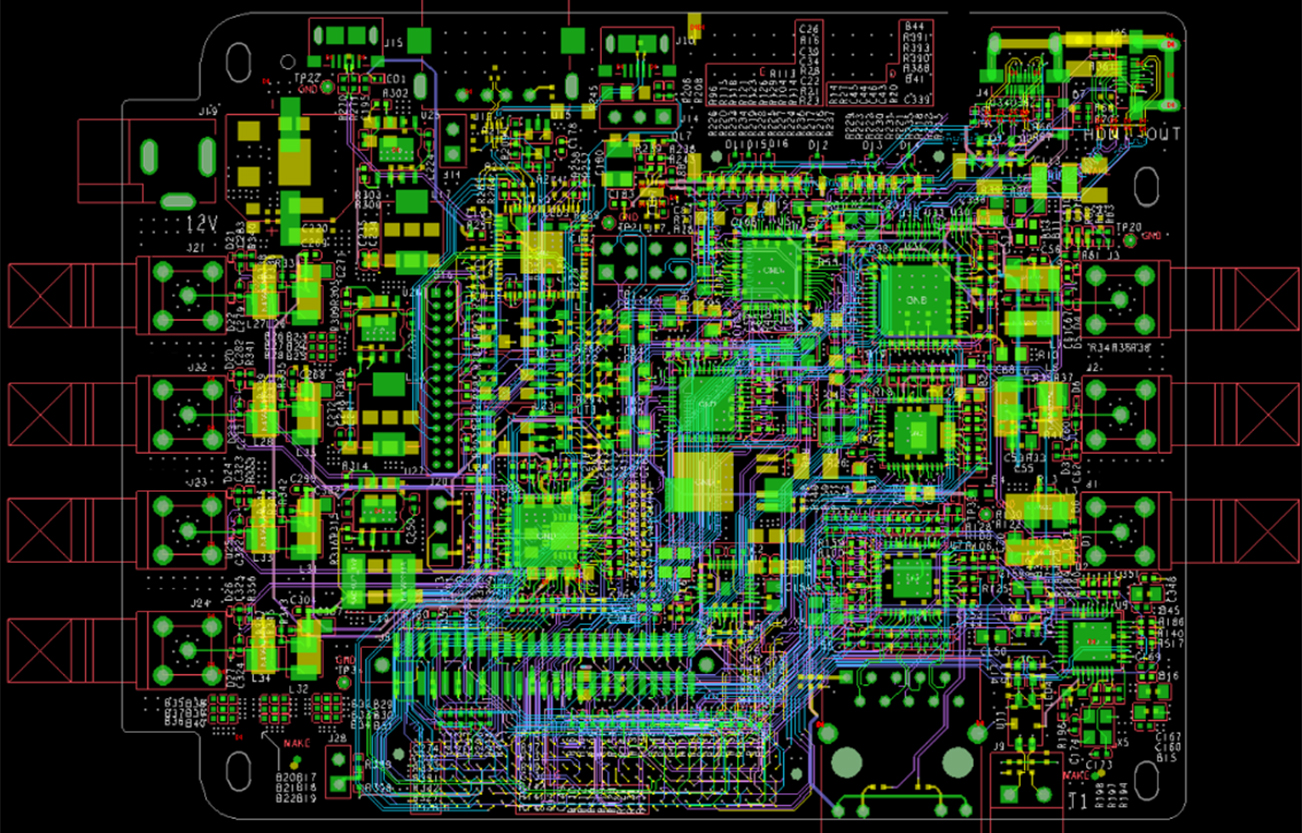
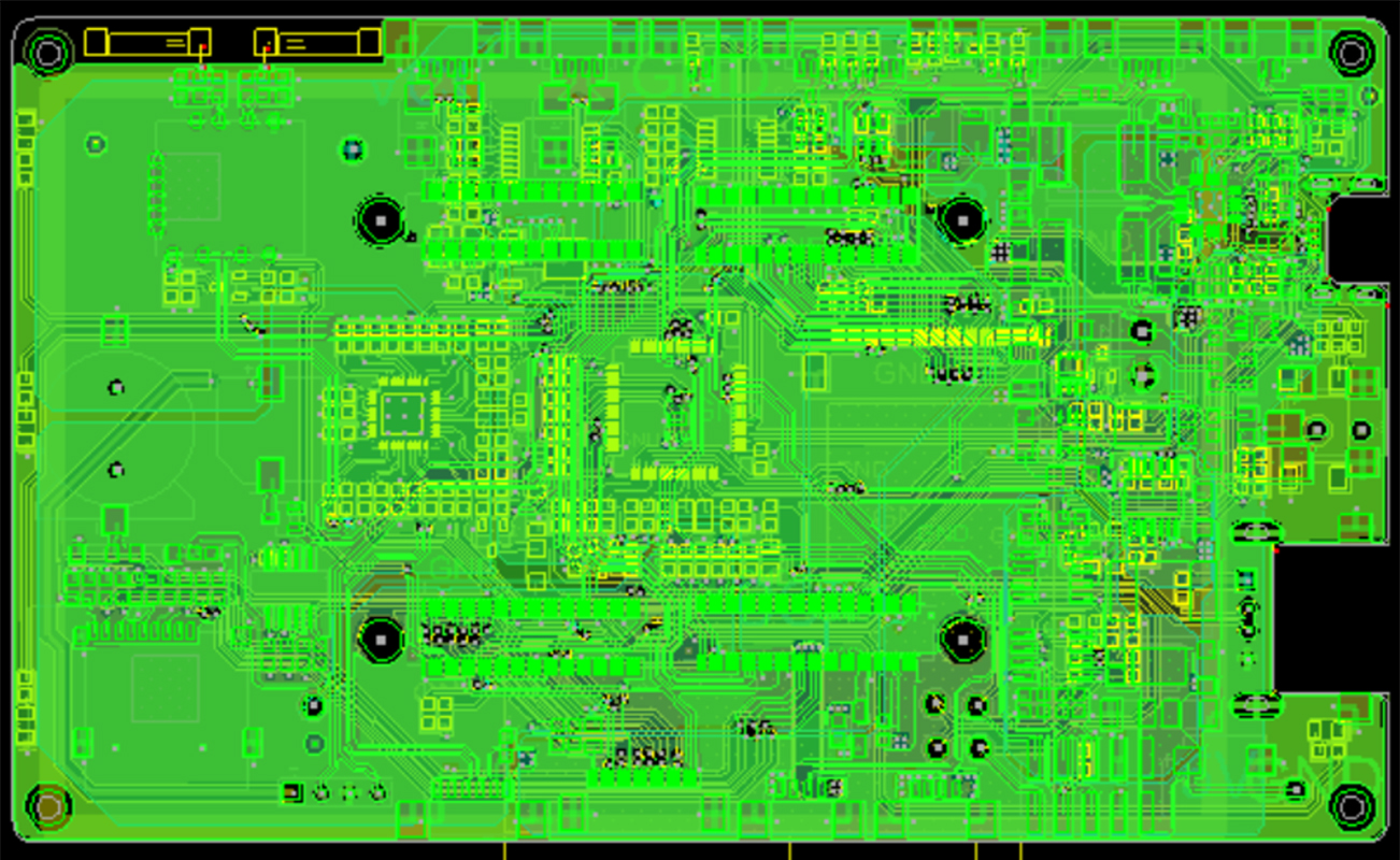
CASE THREE
This case is a high-speed interface conversion motherboard for ADAS product of advanced auxiliary driving system commissioned by an automotive electronics customer
Number of floors: 10
Including: two power planes, including GMSL high-speed digital video signal, HDMI, gigabit network port, serial port to USB, can bus, FPD-link bus, 100-watt DC-DC power module, CVBS composite broadcast signal, etc The project focuses on the complexity of various high-speed signal routing, which has high requirements for PCB design layering planning and routing priority.